Introduction
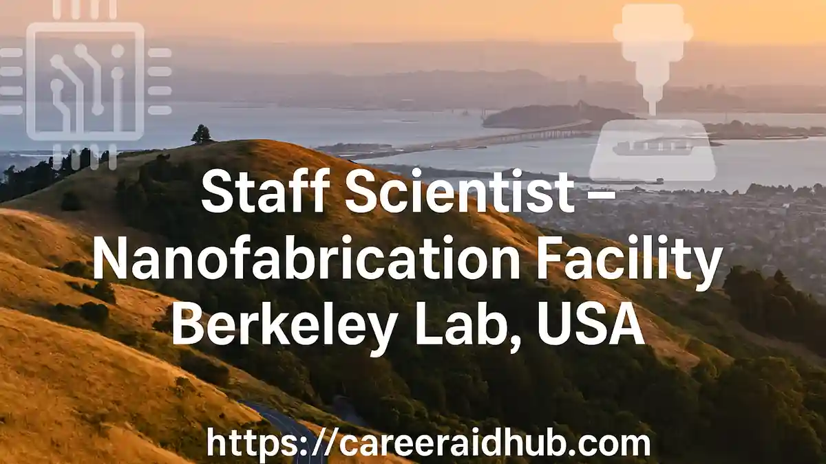
The Molecular Foundry at Lawrence Berkeley National Laboratory (LBNL) invites applications for a Staff Scientist in its Nanofabrication Facility—a uniquely balanced role that combines independent, high-impact research with hands-on support for a global user community. Situated within a premier U.S. Department of Energy (DOE) user facility, the position offers a platform to develop cutting-edge materials and devices for quantum information science while enabling visiting researchers from academia, government laboratories, and industry to execute ambitious experiments. Because it is designed as both a research and service appointment, the role is well suited to scientists who enjoy advancing their own program and, at the same time, helping others achieve first-rate results in a safe, inclusive environment.
This search-friendly guide explains the Berkeley Lab Staff Scientist role in nanofabrication—scope, eligibility, salary, work mode, and key dates—so applicants can prepare a strong dossier. It distills the official details into clear, professional language while keeping the structure intact and the focus on quantum materials and facility-user impact.
Why this role stands out
A dual mandate that accelerates scientific progress
Unlike narrowly defined academic positions, the Foundry’s Staff Scientist model deliberately balances responsibilities: approximately 50% independent research and 50% user support. Consequently, you are not choosing between building a
A user facility with outsized scientific reach
As a DOE user facility, the Foundry supports diverse external users via peer-reviewed access. Therefore, your day-to-day scientific interactions extend beyond your own group. You will collaborate across materials systems, share best practices, and disseminate facility-level improvements that benefit hundreds of users annually. In practice, this means your contributions scale widely and visibly.
Scientific focus: materials for quantum information
Targeting coherence, scalability, and manufacturability
The facility is prioritizing a research program that advances quantum phenomena in materials—in particular, superconducting devices and architectures relevant to quantum computing and quantum sensing. While fundamental insight remains crucial, the agenda also emphasizes device metrics such as coherence, stability, and reproducibility, all of which must improve for scalable quantum technologies.
Tooling and infrastructure to push the frontier
You will have access to advanced thin-film platforms, new QIS cluster deposition capabilities, and ultralow-temperature characterization (including dilution refrigerators and high-field measurements). Because these resources live under one roof, you can connect growth, processing, and cryogenic test in a single, structured workflow. In parallel, data-centric methods—such
What you’ll do (high-level)
1) Lead an independent research program
Define a coherent, multi-year scientific vision aligned with Foundry priorities in quantum materials. Develop hypotheses, design experiments, supervise personnel, and build collaborations that produce measurable advances in device physics and materials processing.
2) Build and sustain a thriving user program
Attract, onboard, and support users from universities, national labs, and industry. Offer practical guidance on lithography, etch, deposition, and integration; maintain transparent documentation; and enable safe, reproducible workflows that translate quickly from prototype to device.
3) Drive cryogenic device characterization
Coordinate robust low-temperature testing—spanning transport, high-field, and microwave measurements—to close the loop between process parameters and device outcomes. Establish standardized test plans and data schemas so users can compare results across projects.
4) Advance superconductor process development
Use the new QIS cluster deposition system to explore materials stacks and interfaces, optimize film quality, and reduce loss mechanisms. Where appropriate, adopt automated data capture so that recipes, metrology, and cryogenic metrics remain linked.
5) Integrate data and enable learning systems
Work with
6) Publish, present, and mentor
Disseminate results through peer-reviewed publications and conferences. Mentor staff, postdocs, and students; cultivate a positive safety culture; and, when applicable, contribute to proposals and external funding.
Who should apply
Profile of a strong candidate
The search considers early-career (career-track) and experienced (career) scientists. Successful applicants typically combine end-to-end device experience—growth, patterning, metrology, and cryogenic test—with a user-oriented mindset and excellent communication skills. If you thrive in collaborative spaces and take initiative to solve cross-disciplinary problems, you will likely find the Foundry a good fit.
Culture and values
The Foundry emphasizes safety, inclusion, openness, and scientific rigor. Staff Scientists model these values by sharing knowledge generously, documenting procedures clearly, and upholding laboratory best practices. Importantly, you will be part of a community whose mission is to enable others to do their best work.
Minimum qualifications
- Doctorate (or equivalent) in physics, chemistry, materials science/engineering, or a closely related field aligned with nanofabrication and nanoscience.
- 5+ years of professional nanofabrication experience, including 3+ years focused on superconducting circuits and/or qubit device fabrication.
- Demonstrated scholarly productivity (talks, publications, patents) with typical expectations on the order of at least one invited or contributedtalk annually and multiple peer-reviewed outputs per year.
- Proven user-support orientation—clear communication, collaborative problem-solving, and respectful engagement with diverse teams.
- Process/tool proficiency spanning e-beam lithography, RIE/ICP etch, ALD, e-beam evaporation, sputtering, integrated UHV systems, and rigorous safety practice.
Desired profile
- Experience running or overseeing ultralow-temperature experiments (e.g., dilution refrigeration, transport under high fields) with careful noise control and low-background techniques.
- Leadership in nanoscience across academic or industrial environments; strong analytical judgment; and a compelling, well-articulated scientific vision.
Application package
Required documents
- Curriculum Vitae;
- Research Statement (≈3 pages) detailing your near-term plan and long-term vision;
- User Support Statement (≈1 page) explaining how you will strengthen the Foundry’s DOE user mission—through training, documentation, safety stewardship, and scalable best practices.
How reviewers assess your file
Committees look for a coherent research narrative, evidence of facility-level impact, and the ability to guide users to successful outcomes. They also value documented improvements to processes or instrumentation that others can adopt.
Key dates & appointment type
Timeline (month–year only)
- Priority review: Dec 2025 (submit early for full consideration).
- Next cycle (anticipated): Oct–Dec 2026 — we will update soon (window based on typical annual search rhythms for similar roles at the Foundry).
Appointment and conversion
- Type: Full-time career-track term of two years, renewable up to five years, with the potential for conversion to a career appointment subject to performance, funding, and operational needs.
- Flexibility: Depending on experience, exceptionally qualified candidates may be considered directly for a career Staff Scientist appointment.
Compensation & work mode
Salary and benefits
- Expected salary range: $129,924 – $207,900. The broader salary band for the role extends up to $311,820, with final placement determined by qualifications, experience, and internal equity.
Location, schedule, and access
- Primary worksite: 1 Cyclotron Road, Berkeley, CA.
- Modality: Predominantly on-site (generally 4+ days/week), with occasional remote work as operational needs allow.
- Access: Valid REAL ID or equivalent identification is typically required for site entry.
About the Molecular Foundry & the Nanofabrication Facility
The Foundry at a glance
The Molecular Foundry is one of five Nanoscale Science Research Centers within the DOE complex. It provides peer-reviewed user access, specialized staff expertise, and integrated toolsets that span synthesis, patterning, characterization, and theory. As a staff member, you help maintain the Foundry’s high standards of safety, reliability, and scientific excellence.
Capabilities of the Nanofabrication Facility
The Nanofabrication Facility supports device fabrication over a broad range of materials, with particular depth in superconducting devices and quantum-relevant processing. Its tooling—from advanced lithography and dry etch to multilayer deposition and cryogenic test—enables complete process-integration studies. Because these capabilities are tightly linked, the facility is ideal for correlating materials growth, patterning, and low-temperature device performance.
How to apply
Submit your application via Berkeley Lab Careers. Prepare your documents in PDF, use clear file names, and ensure each statement addresses the role’s quantum-materials emphasis and the user-facility mission. For the user statement in particular, outline how you will onboard users efficiently, maintain excellent safety records, and scale knowledge through documentation and training. You should also highlight any prior success supporting shared facilities, including published protocols, recipe libraries, or instrument upgrades.
- Official posting: Staff Scientist – Nanofabrication Facility (Molecular Foundry), Berkeley Lab.
Tips to strengthen your application
Clarify a 3–5-year vision (with milestones)
Explain how your research will improve key quantum-device metrics (e.g., coherence and stability). Tie milestones to specific process improvements, measurement campaigns, or collaborations. Where appropriate, propose cross-facility experiments that integrate thin-film growth, patterning, and cryogenic characterization.
Demonstrate user-facility impact
Show how you will grow the user base and raise overall outcomes. For example, propose onboarding templates, “starter kits” for recurring device types, or standardized cryogenic test plans that reduce ramp-up time and improve data comparability across projects.
Connect process to performance with data
Document how you will capture process history, metrology, and low-T metrics in a unified schema. As feasible, describe ML-assisted approaches that can predict device quality from recipe parameters. This kind of rigor positions the facility—and your program—for repeatable gains.
Highlight mentoring and team science
Provide concrete examples of training students, postdocs, and users. Mention collaborations that led to publications, patents, or facility upgrades; emphasize your ability to coordinate multi-stakeholder efforts safely and efficiently.
Quantify your record
Use numbers to establish momentum: invited talks, publications per year, patents, external awards, or successful proposals. These indicators help reviewers gauge your readiness for both independent science and user leadership.
Equal opportunity & background check
Berkeley Lab is an Equal Opportunity Employer. Evaluation of conviction history focuses on relevance to the position; a prior conviction does not automatically disqualify a candidate. The Lab supports a respectful, inclusive workplace, and all applicants are encouraged to apply based on their ability to meet the role’s scientific and operational requirements.
Quick reference
- Role: Staff Scientist – Nanofabrication Facility (Molecular Foundry, LBNL)
- Focus: Materials for quantum information; superconducting device fabrication & cryogenic characterization
- Balance: ~50% independent research / ~50% user support
- Location: Berkeley, CA (primarily on-site)
- Salary (expected): $129,924 – $207,900 (full range up to $311,820)
- Priority review: Dec 2025
- Next cycle (anticipated): Oct–Dec 2026 — we will update soon
- Apply: Via Berkeley Lab Careers (official posting)
Feature Details
Feature | Details |
Program Name | Staff Scientist – Nanofabrication Facility (Molecular Foundry, Berkeley Lab) |
Host Country | United States (Bay Area/California) |
Funded By | Lawrence Berkeley National Laboratory (U.S. Department of Energy) |
Duration | Two-year career-track term, renewable up to five years, with potential conversion to career |
Study Mode | Full-time, primarily on-site (limited hybrid flexibility as operations allow) |
Eligibility | Ph.D. (or equivalent) in a relevant field; extensive nanofabrication experience; user-support orientation |
Financial Support | Salary expected range $129,924 – $207,900; broader band up to $311,820 (final placement depends on qualifications/experience) |
Fields of Study | Nanofabrication, superconducting devices, quantum computing/sensing, thin-film growth, cryogenic characterization |
Deadline | Dec 2025 (priority review) — we will update soon |
Official Website | Click here |
Conclusion
This position offers a rare combination of independent discovery and community impact in a world-class DOE user facility. If your expertise spans superconducting device fabrication, cryogenic characterization, and user-centric operations—and you want your work to influence a broad community—then this role will let you lead science while enabling others to excel. For complete, authoritative details and to apply, refer to the official Berkeley Lab posting.
Frequently Asked Questions (FAQs)
Typically, you lead independent quantum materials research and simultaneously support external users with processes, documentation, safety, and training inside the Molecular Foundry.
Generally, it’s a full-time career-track term with potential conversion to career status, subject to performance, funding, and operational needs.
Typically, candidates hold a Ph.D. in relevant fields and bring deep nanofabrication experience, including superconducting devices, e-beam lithography, RIE/ICP etch, ALD, sputtering, and cryogenic characterization.
Generally, responsibilities split about half independent research and half user support; however, exact percentages may vary with projects and facility priorities.
Primarily, you work on-site in Berkeley four or more days weekly; however, limited remote work may occur depending on operational needs and schedules.
First, articulate a 3–5-year quantum-materials plan, milestones, key tools, collaborations, and expected device metrics; additionally, explain data workflows linking process parameters to performance.
Briefly, show how you will onboard users, document recipes, train safely, standardize cryogenic tests, and, furthermore, scale knowledge through playbooks, seminars, and open protocols.
Yes, international candidates may apply; however, you must hold appropriate work authorization, and potential sponsorship follows institutional policy and U.S. regulations.
Typically, the lab publishes an expected salary range and a wider full range; moreover, final offers depend on experience, skills, and internal equity.
Therefore, submit before the priority review date; meanwhile, applications usually remain open until the posting closes or the position fills.